Disclaimer:
The contents of this article are purely engineering and technical reference. It is not a product specification or guarantee but a concentration on physical and optical processes of TFT LCD water ripple phenomenon.
1. What Is the TFT LCD Water Ripple Phenomenon?
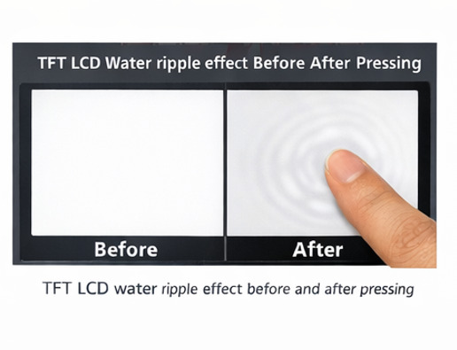
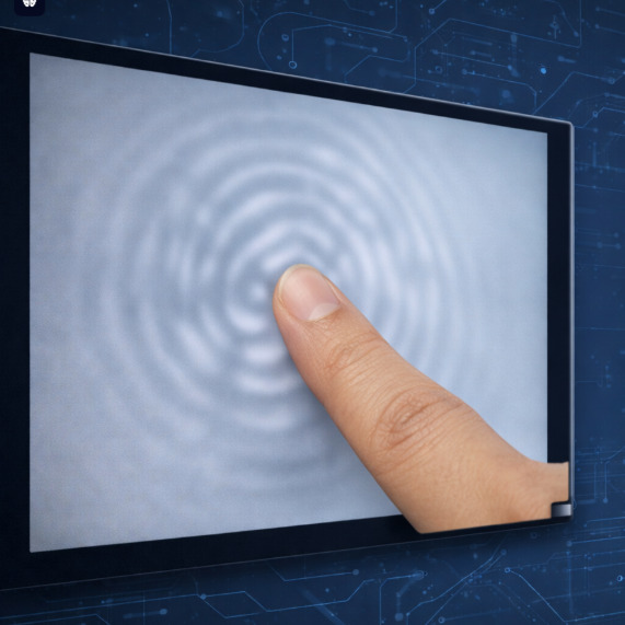
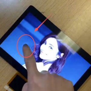
An optical and stress-related non-uniformity and not electrical or pixel defect, water ripple in TFT LCD displays. It is reflected in the cycle of changes in brightness or grayscale and it resembles waves, rings, or discontinuous interference patterns on the display surface.
1.1 Key Characteristics:
-
Visibility: Most noticeable on low-gray (Gray 30–80) or full-white backgrounds. This effect depends on the viewing angle, brightness of the display and the ambient light.
-
Stress Sensitivity: Appears or intensifies under mechanical stress, such as pressing, frame fixation, or adhesive shrinkage. When the stress is relieved it may vanish to some extent.
-
Application Specificity: Often observed only after final device assembly, since module-level inspections may not detect minor variations.
This phenomenon is especially critical in industrial, medical, and automotive applications, where display uniformity is essential for user safety, product reliability, and perceived quality.
1.2 Does Water Ripple Only Appear When Pressing the Screen?
This is one of the most common misunderstandings.
In engineering practice, a more accurate statement is:
The TFT LCD water ripple effect is most easily observed when pressing the screen, but it does not only exist under pressing conditions.
Screen pressing is simply the most direct and repeatable way to introduce vertical mechanical stress, which makes the ripple effect more visible. However, the phenomenon may also appear without any user interaction.
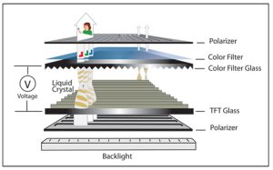
2. Core Mechanisms Behind Water Ripple
The phenomenon of water ripple is a result of a combination of various factors, among them being the uniformity of the liquid crystal layers, the stress of the material, optical characteristics, and mechanical design.
2.1 Cell Gap Variations
Even the slight variations in the liquid crystal thickness (+-0.1-0.2 mm) can cause phase delays in the transmission of light, causing visible interference patterns of polarized light.
Causes include:
-
Uneven spacer distribution or partial collapse.
-
Irregular liquid crystal curing or shrinkage during injection.
-
Imperfect glass substrate flatness (warp or bow).
2.2 Stress-Induced Birefringence
Mechanical stress from screws, frame pressure, or adhesive shrinkage can change the local refractive index, altering grayscale response and creating visible patterns. This effect is very dynamic; the intensity of the ripple can vary with the pressure or variation of temperature.
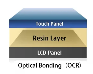
2.3 Residual Stress from Polarizer Bonding
Long term residual stress areas can be generated during lamination of polarizers with unbalanced adhesive thickness, misalignment or tension differences. These areas can enhance the ripple of water in certain gray levels or brightness without the external force.
2.4 Backlight Amplification
Backlights do not give rise to water ripple, but can make it more visible:
-
LEDs with high brightness bring an increase in contrast so minor ripples can be visible.
-
Point-source LGPs can emphasize interference patterns.
-
Inadequate diffusion layers or low haze may reduce uniformity, indirectly increasing perceived ripple.
3. Typical Triggers and Amplifiers
Water ripple visibility is influenced by several operational and environmental factors:
-
Temperature: Wide operating ranges (-20°C to +70°C) may induce thermal stress due to material expansion coefficient mismatches.
-
Time/Aging: Long-term mechanical creep releases residual stress, gradually increasing ripple.
-
Assembly: Localized pressure during final assembly, especially at corners or screw points, can exacerbate ripple.
-
Display Content: Light backgrounds or low-gray UIs accentuate ripple visibility.
Such knowledge of these triggers enables the engineer to anticipate any ripple problems when developing and testing a product.
4. Bonding Method and LCD Mode Impact
Bonding method and panel type are matters that cause a strong influence on visibility of water ripple.
| Combination | Observed Risk | Explanation |
|---|---|---|
| TN + Optical Bonding (Full Lamination) | High | Pressure transfers directly to LCD, clear ripple under low-gray or bright backgrounds. |
| TN + Air Bonding (Frame Bonding) | Low | Mechanical buffer disperses pressure; ripple is barely visible. |
| IPS + Any Bonding | Very Low | IPS molecules rotate mainly in-plane, minimizing stress sensitivity. |
Case Study:
In a recent 7-inch project, a TN panel with full optical bonding exhibited distinct water ripple under light pressure. Switching to frame (air) bonding almost completely eliminated visible ripple, illustrating the importance of mechanical design and bonding method in ripple mitigation.

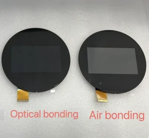
TN panel + Optical bonding TN Panel+Air bonding
5. Differentiation from Mura and Light Leakage
Engineering teams often confuse water ripple with other display issues such as Mura or light leakage. The accurate identification is essential to problem solving.
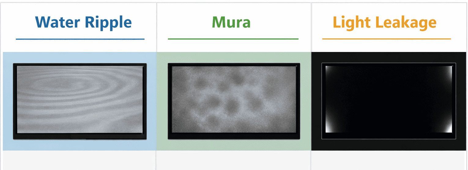
| Feature | Water Ripple | Mura | Light Leakage |
|---|---|---|---|
| Appearance | Waves, rings, interference patterns | Cloudy or blotchy uneven brightness | Edge bright bands or localized whitening |
| Cause | Optical interference + stress | Process-induced brightness variation | Structural sealing defects or backlight leakage |
| Stress Sensitivity | Yes | No | Partially |
| Electrical Issue | No | No | No |
6. Design and Application Recommendations
Operational Guidelines
-
Avoid concentrated pressure on active display areas.
-
Use soft or distributed touch methods during testing.
Mechanical Design
-
Reinforce the frame or housing to disperse stress, especially for full-lamination panels.
-
Consider corner supports or pressure buffers to reduce localized force transfer.
Panel and Bonding Selection
-
Prefer IPS panels for high uniformity.
-
For TN panels, air bonding is recommended to minimize ripple.
-
Optical bonding may be necessary for touch sensitivity but requires careful stress management.
Testing Recommendations
-
Evaluate ripple after full device assembly, not just at the module level.
-
Use low-gray or white test patterns under simulated operational pressures.
-
Monitor over temperature ranges and under long-term operation.
7.FAQ – Design Considerations
Q1: Is water ripple a display defect?
No, it is an optical-structural effect, not an electrical failure.
Q2: Does water ripple only appear under pressing?
Mostly yes, though residual stress can make minor ripple visible without pressure.
Q3: Why is TN more prone than IPS?
TN molecules are highly sensitive to vertical stress; IPS molecules rotate in-plane and resist stress-induced optical changes.
Q4: Does optical bonding increase ripple risk?
Yes, particularly on TN panels, because pressure transmits directly to the liquid crystal layer.
Q5: Can air bonding reduce ripple?
Yes, it provides a mechanical buffer, dispersing pressure and reducing visibility.
Q6: Does backlight cause ripple?
No, but high-brightness backlights can amplify already existing ripple patterns.
Q7: How should ripple be evaluated during development?
Test after full assembly using low-gray or white backgrounds, applying light pressure tests.
Q8: Can ripple be completely eliminated?
Not entirely. Proper panel selection, bonding method, and mechanical design can reduce ripple to nearly imperceptible levels.
8. Conclusion
TFT LCD water ripple is a typical optical-mechanical issue, influenced by:
-
Panel type (TN vs IPS)
-
Bonding method (optical vs air)
-
Cell gap uniformity
-
Mechanical and assembly stress
Knowing about these factors enables the engineers to optimize the design, verify assembly and use suitable panels, reducing the visibility of ripple and providing high display uniformity in industrial, medical, or automotive applications.
By designing, selecting the panel, optimization of bonding method and extensive testing, it is possible to ensure that the water ripple is minimized to undetectable levels without affecting functionality or appearance.