CTP Technologies
Capacitive touch screens are made of single or multiple layers of material that are coated with a conductor such as Indium Tin Oxide. A protective cover seals the assembly off from the environment.
When another electrical conductor, like a bare fingertip or a stylus, touches the surface, an electric circuit is completed at that location. Sensors embedded in the glass then detect the location of the flow of current, which is then registered as a touch event.
This is different from the way that resistive touch technology works, where physical pressure is involved.
Capacitive touch technology can be divided into:
Surface Capacitive
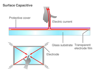
Transparent conductive coating is on the base glass sheet, and glass protective coating is placed over it. Electrodes are placed on the four corners. The same phase voltage is imposed to the electrodes on the four corners, then a uniform electric field will be forming over the panel. When a finger touches on the panel, electrical current will flow from the four corners through the finger. Ratio of the electrical current flowing from the four corners will be measured to detect the touched point. The measured current value will be inversely proportional to the distance between the touched point and the four corners.
Features:
◆ Surface capacitive technology is suitable for large size monitors.
◆ Surface capacitive sensor can respond to light touch, and no pressure force is needed for detection
◆ Visibility is high because structure is only one glass layer.
◆ Surface capacitive is structurally tough as it is made of one sheet of glass.
◆ Surface capacitive does not get affected by moist, dust, or grease.
◆ Parallax is minimized in surface capacitive.
◆ Surface capacitive has high resolution and high response speed.
◆ Basically, surface capacitive can detect touches by fingers only. It does not detect input by gloved hand. Some surface capacitive touch screens may detect touches by thin-gloved hand, but they do not support the combination use of bare finger and gloved finger. Some surface capacitive touch screens support pen writing, but they usually does not support combination use of finger touch and pen writing.
◆ Surface capacitive technology does not support multi-touch.
◆ Surface capacitive touch screen is likely to be affected by noise. Recently, tolerance for noise has been improved with various methods such as noise shielding.
Projected Capacitive
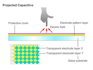
Projected capacitive touch panels are often used for smaller screen sizes than surface capacitive touch panels. The internal structure of these touch panels consists of a substrate incorporating an IC chip for processing computations, over which is a layer of numerous transparent electrodes is positioned in specific patterns. The surface is covered with an insulating glass or plastic cover. When a finger approaches the surface, electrostatic capacity among multiple electrodes changes simultaneously, and the position were contact occurs can be identified precisely by measuring the ratios between these electrical currents.
There are two types of sensing methods in projected capacitive technology. They are GRID type and wire sensing type. GRID type will be introduced here. Human body is conductive since it contains a lot of water. When a finger comes close to the patterning of X and Y electrodes, a capacitance coupling will occur between the finger and the electrodes. The capacitance coupling makes the electrostatic capacitance between the X and Y electrodes change. The touch sensor detects touched points as it checks where on the electrode lines the electrostatic capacitance changed.
Features:
◆ Projected capacitive supports multiple touches, thus supports various elaborate inputs.
◆ Projected capacitive has relatively long life because it has no moving parts in operation.
◆ Projected capacitive has high durability.
◆ Sensitivity of the sensor can be adjusted. If sensitivity is adjusted to high level, the touch screen can be operated over a cover glass or cover plastic sheet. These cover sheets provide additional durability, environmental resistance, and a lot of flexibility in design.
◆ If sensitivity is increased, projected capacitive can be operated with gloved fingers.
◆ Projected capacitive touch screen is excellent at optical property.
◆ Projected capacitive responds to light touch. No pressure force is needed for detection.
◆ Projected capacitive requires an advanced technology to measure electrostatic capacitance and achieve precise locational information from it. Unlike resistive technology, it does not work simply by connecting a touch screen with a controller sourced from somewhere. A projected capacitive touch screen and controller need to be designed together.
◆ Projected capacitive is susceptible to electrical noise due to its detection mechanism. Noise from LCD is especially influential to the sensor. Recently, various methods are developed to improve tolerance for noise.
◆ Projected capacitive requires fine pattering, thus takes high processing cost.
Self-Capacitance
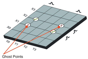
Self-Capacitance is based on measuring the capacitance of a single electrode with respect to ground. When a finger is near the electrode, the human-body capacitance changes the self-capacitance of the electrode. In a self-capacitance touch screen, transparent conductors are patterned into spatially separated electrodes in either a single layer or two layers. When the electrodes are in a single layer, each electrode represents a different touch coordinate pair and is connected individually to a controller. When the electrodes are in two layers, they are usually arranged in a layer of rows and a layer of columns; the intersections of each row and column represent unique touch coordinate pairs. However, self-capacitance touch-screen controllers do not measure each intersection; they only measure each row and column;
This works well when only a single finger is touching the screen. For example, As shown in the below picture, a single-finger touching location X2,Y0 can be sensed accurately by measuring all the X electrodes and then all the Y electrodes in sequence. Measuring individual electrodes rather than electrode intersections is the source of one of the major disadvantages of two-layer self capacitance touch screens – the inability to unambiguously detect more than one touch. Two fingers touching in locations X2,Y0 and X1,Y3 produce four reported touch points. However, this disadvantage does not eliminate the use of two finger gestures with a self-capacitance touch screen. The secret is in software – rather than using the ambiguous locations of the reported points, software can use the direction of movement of the points. In this situation it does not matter that four points resulted from two touches; as long as pairs are moving away from or toward each other (for example), a zoom gesture can be recognized.
Mutual Capacitance
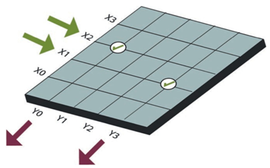
Mutual Capacitance is a more common type of pro-cap today, which allows an unlimited number of unambiguous touches, produces higher resolution, is less sensitive to EMI, and can be more efficient in its use of sensor space. Mutual capacitance makes use of the fact that most conductive objects are able to hold a charge if they are very close together. If another conductive object, such as a finger, comes close to two conductive objects, the charge field (capacitance) between the two objects changes because the human-body capacitance “steals” some of the charge.
In a mutual-capacitance touch screen, transparent conductors are always patterned into spatially separated electrodes in two layers, usually arranged as rows and columns. Because the intersections of each row and column produce unique touch-coordinate pairs, the controller in a mutual-capacitance touch screen measures each intersection individually (see right Fig). This produces one of the major advantages of mutual-capacitance touch screens – the ability to sense a touch at every electrode intersection on the screen.
Because both self-capacitance and mutual capacitance rely on the transfer of charge between human-body capacitance and either a single electrode or a pair of electrodes, this method of capacitive sensing is most commonly called “charge transfer.”
Optical donding
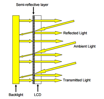
Optical bonding is a type of integration service that is used to laminate the touch screen (or other rigid material) to the top surface of the LCD. The bond is created by dispensing and then curing a form of optically clear adhesive between the touch screen and display forming a permanent bond with no air gap between the two components. There are many benefits to the optical bonding method of integration vs. traditional gasket attach methods, one of the most notable being the enhanced optics and improved impact strength.
Advantages:
◆ Improved transmission by removing internal reflections between the LCD and touch sensor glass.
◆ Improved viewing in bright ambient light conditions.
◆ Less power required to make the backlight brighter in high ambient or even normal viewing conditions.
◆ Can improve mechanical performance.
◆ Can provide better impact, shock and vibration resistance for units that require a rugged environment.
◆ Elimination of any dust, dirt, or moisture that can collect between the sensor and display surfaces.
◆ Low haze and low yellowing fill material.

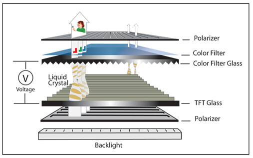 TFT (Thin-Film Transistor) Displays are active-matrix LCDs with full RGB color screens. These screens feature bright, vivid colors and have the ability to show fast animations, complex graphics and crisp custom fonts. TFTs are perfect displays for providing a rich user interface for all types of products. While typically used in consumer devices like personal DVD players and handheld devices, TFTs are also well suited for industrial application.